Engineering leader · Precision test & measurement systems
I build teams and systems that recover the most difficult signals.
Engineering leader with a PhD in physics. I lead precision measurement equipment from architecture, hardware, software and calibration algorithms through to installation in customer production, and stay hands-on in the hard technical calls. My foundation is measurement science: knowing where noise and error come from, and proving a result is real. I'm ready for the next challenge.
What I do
Four engineering pillars that feed each other.
A tool isn't finished until measurement proves it. Measurement data sets the process recipe, the process's needs set the spec for the next tool, and sales engineering turns a proven tool into an order.
Architecture, hardware, control software and calibration algorithms, through installation and troubleshooting.
Test & measurementMeasurement science: noise, calibration, correlation and validation, turned into decisions.
Process engineeringDevelop and qualify the processes that run on a tool, from recipes to designed experiments.
Sales engineeringTake proven tools to customers, from evaluation to acceptance.
Featured projects
Three measurement systems, start to finish.
Photonic wafer test · 2023 – now
An automated photonic wafer prober, from first specification to production
System architecture, hardware, control software and patented calibration algorithms for an automated photonic wafer prober, through installation in customer production.
Read the case study →Spintronics · NTU · 2017 – 2021
Reading a single skyrmion electrically
A picoamp tunnelling measurement to read each nanodot’s bit, a skyrmion as 1 or none as 0, by non-collinear magnetoresistance. Designed, validated step by step and run on 300–400 nm dots, ending in a clear verdict that set the next device batch.
Read the case study →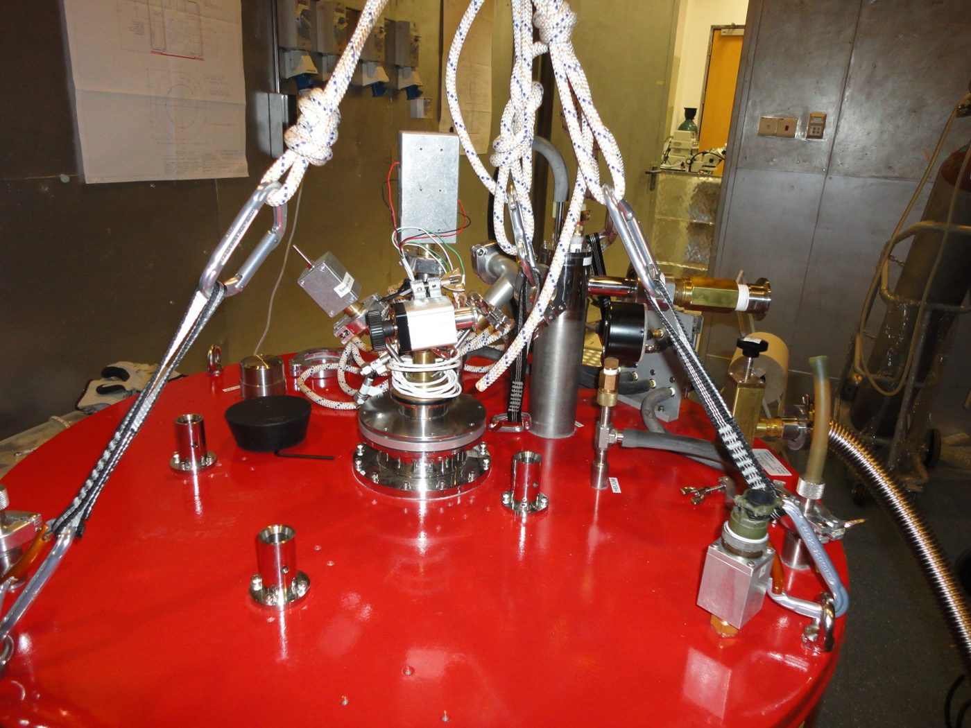
PhD · NTU · 2009 – 2014
A nanovolt measurement system that found a hidden superconducting surface
Two homebuilt dipper cryostats with a pumped 2 K pot, automated in LabVIEW: measurement noise below ±3 nV, and a surface transition up to 64% above the bulk, published and patented.
Read the case study →Special expertise
The expertise behind these systems.
Test automation
Instruments, sequencing and data in one programLabVIEW measurement systems and production control software for a wafer prober.Active thermal control
Dipper cryostats, 300 K down to 2 KThermal architecture, calibrated sensors, PID loops and thermal debug.Vacuum
High vacuum in the cryostats I builtVacuum cans and pumped sample spaces for my cryogenic probes.High-speed test
Bandwidth, eye diagrams and BEROn-wafer RF bandwidth of photodiodes, and the eye-diagram and BER plan for 224 Gb/s.