Projects
Three measurement systems, start to finish.
Photonic wafer test · 2023 – now
An automated photonic wafer prober, from first specification to production
System architecture, hardware, control software and patented calibration algorithms for an automated photonic wafer prober, through installation in customer production.
Read the case study →Spintronics · NTU · 2017 – 2021
Reading a single skyrmion electrically
A picoamp tunnelling measurement to read each nanodot’s bit, a skyrmion as 1 or none as 0, by non-collinear magnetoresistance. Designed, validated step by step and run on 300–400 nm dots, ending in a clear verdict that set the next device batch.
Read the case study →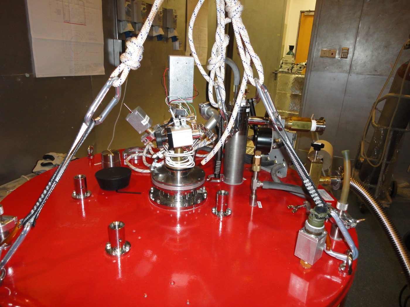
PhD · NTU · 2009 – 2014
A nanovolt measurement system that found a hidden superconducting surface
Four generations of cryogenic probe, measurement noise below ±3 nV, and a surface transition up to 64% above the bulk, published and patented.
Read the case study →Special expertise
The expertise behind these systems.
Test automation
Instruments, sequencing and data in one programRecipe-driven runs, settle-before-measure gating and full raw-data logging, from LabVIEW to production software.Active thermal control
Closed-loop temperature control from 300 K to 2 KThermal architecture, calibrated sensors, PID loops and thermal debug, from my cryogenic test systems.Vacuum
High vacuum in the cryostats I builtVacuum cans and pumped sample spaces for my cryostats.High-speed test
Bandwidth, eye diagrams and BEROn-wafer RF bandwidth, eye diagrams, PAM4 and bit error ratio.